|

Abstract
Part 1
Mathematics, Logic & Computers
1.1 Mechanical computers
1.2 Abstract mathematics
1.3 Boolean logic
1.4 Reducing mathematical relationships to abstract
Boolean logic
1.5 Physical implementation of Boolean logic
1.6 Universal computation
Part 2
Cellular
Automata Computers
2.1
Basic structure and operation of a
CA
2.2 Useful things to do with a CA
Part 3
Banks'
Proof of Universality in 2-dimensional, 5-neighborhood CA
3.1 Rules of change
3.2 The wire and signal
3.3 The dead end
3.4 The fan out junction
3.5 The clock
3.6 The logic element
3.7 The NOT gate
3.8 The NOR gate
Part 4
Epilog
4.1 Manipulation of information by
whatever means
4.2 The machine
within the machine
4.3 The
dependent automaton
4.4 Progress in understanding computers and cellular
automata
Back to abstract
Go to BottomLayer home
|
|
Commentary on Edwin Roger Banks, "Information
Processing and Transmission in Cellular Automata,"
Banks' Ph.D. thesis, 1971 (MIT, Dep't of Mechanical
Engineering). By Ross Rhodes.
|
Part 3
Banks'
Proof of Universality in 2-dimensional, 5-neighborhood Cellular
Automata
Working with Edward Fredkin at MIT, Banks' assignment was to simulate with a cellular automata network the inner workings of the standard general purpose computer of the day (and of our day), which consisted of the wires and switches we have illustrated above. The theory was that if Banks could create a cellular automata that would carry signals along defined paths (like an electrical signal carried along a wire), and have these signals interact in the manner of a logic gate to produce a single output based on the character of the input signals, then he would have fully simulated the inner workings of a general purpose universal computer. Having achieved that, he would have thereby proved that his cellular automata could do anything that the hard-wired machine could do to process the information represented by the signals. This is the way Banks puts it:
"To show that a set of transition rules [devised for a checkerboard-like cellular automata array] is computation universal we will illustrate that we can embed a general purpose computation system in the array. That is, there is some configuration of states which can simulate the computer system.
"The direct approach is used. Since a computation system can be physically built out of wires, transistors, etc[.], it will be sufficient to show that there are configurations (initial assignments of states to the cells) that act like wires, etc., which can be interconnected to form the computation system." Banks at 13.
3.1 Rules of Change
Banks begins by defining three transition rules for his checkerboard-like cellular automata. (We may guess that these three rules are actually the result of a very tedious process of trial-and-error.) Banks' three transition rules are all that will be necessary for the entire system - understanding that these three rules will govern the conditions under which the state of the cell will change. If one of the three conditions is not met, the cell will retain its previous value, i.e., it will not change. We will see how the application of these three rules will cause patterns of behavior that will mimic the operations of the familiar universal computer on our desktop.
The three rules formulated by Banks are these: [note 4]
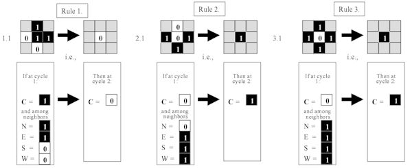
Fig. 3.1.1 The three rules of transition used by
Banks.
Note here that the three rules are valid in each of the four orientations. That is, the rule is valid when the positions of the neighbors are rotated around the cell. So, for example, Rule 1 implies three other rules, as follows:
|
|
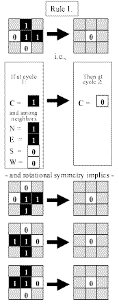
Fig. 3.1.2 Rule 1 and its implied rotations.
|
Using these three rules, with their implied rotations, Banks sets out to determine whether he can build wires that can carry signals to logic gates by creating specific configurations of the checkerboard.
|
3.2 The wire and signal.
If we are attempting to simulate on the checkerboard a computer made out of wires conducting electricity, which lead in to logic gates that spit out an output based on the values of the inputs, then we must begin with a "wire" that can carry a "signal" analogous to a copper wire carrying an electrical pulse.
It turns out this can be accomplished with the foregoing three rules by creating a "wire" of three rows of cells that have the value "1." When we place a "signal" consisting of two diagonal cells in the "0" state somewhere along this wire, the three rules cause something extraordinary to happen: the rules cause changes to occur in such a way that both elements of the "signal" disappear from their original
location - and reappear next door! To the observer, it appears that the signal moves one cell at a time to the right along the "wire"! Look at the "wire" below, with the two-cell "signal," and apply the three rules to guess what each cell will look like at the next cycle.
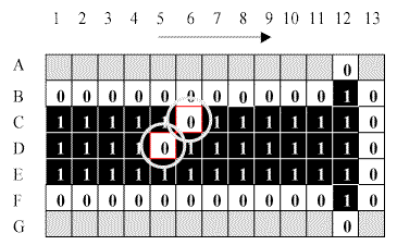
Fig. 3.2.1 The wire (with dead end) and signal.
|
| Cell [C6] evaluates itself and its four neighbors as
shown here, which is the situation of Banks' Rule 2. |

Fig. 3.2.2 Detail of cell [C6]
|

Fig. 3.2.3 Detail of cell [C7], the eastern
neighbor
|
At the same time, it's neighbor to the east,
cell [C7], will evaluate itself as
shown here, which is a rotated version of Banks' Rule 1. |
| Accordingly, on the next cycle, cell
[C6] will change from value "0" to value "1," as dictated by Rule 2. |
(Banks has set up his rules so that the rotation makes no difference to the cell's behavior.) Accordingly, this cell will follow Rule 1, so that on the next cycle this cell will change from value "1" to value "0."
|
|
To the observer, these rules will make it appear that the white cell
[C6] has moved one space to the
right at the next step of the CA.
Following Banks' three rules (with appropriate rotations), you can see that the same thing will happen with cell
[D5]: the original cell will change to
black (Banks' Rule 3), while it's neighbor to the east will change to
white (Rule 1), thereby making it appear that the cell has "moved" to the right. Consequently, we see that the two-cell "signal" appears to move along the wire, and that it will continue to do so as long as the "wire" continues as three rows of black cells bounded by a row of white cells.
And so Banks has created within his cellular automata the wire that can carry a signal - thus simulating one of the necessary components of a desktop computer.
Note that the signal travels on one side of the wire, and the direction of travel is determined by the relative orientation of the two "0"
white cells to each other. The side and the direction are indicated in Banks' diagrams by an arrow along the signal side of the wire, pointing in the direction of travel.
[note 4.1]
3.3 The dead end.
If you follow the signal to the end of the wire illustrated above, applying Banks' three rules, you will see that the
bump-extension at the end of the wire will kill the signal - i.e., white cells in the next-to-last column of the wire will change to black, but their easterly neighbors in the last, extended column will
not change to white. Which is to say the signal will die out when it reaches the next-to-last column.
|
|
Fig. 3.3.1 Animation of signal traveling on wire
(click to open)
|
Here is an animation of the application of Banks' rules to a
"signal" traveling on a "wire" until it meets a
"dead-end," as discussed above.
[Click on the graphic to open the animation.]
[Click here to
open a step-by-step PDF.]
|
3.4 The fan out junction.
Banks devised a fan out junction to split an incoming signal into three branches. As a bonus, it turns out that Banks' three rules cause behaviors at the junction that allow interaction with incoming signals from the branches. Consequently, this fan out junction is the basis of the logic element that Banks will demonstrate.
This is what Banks' fan out junction looks like. The signal comes in from the left (in the illustration), and proceeds out each arm - north, east, and south.
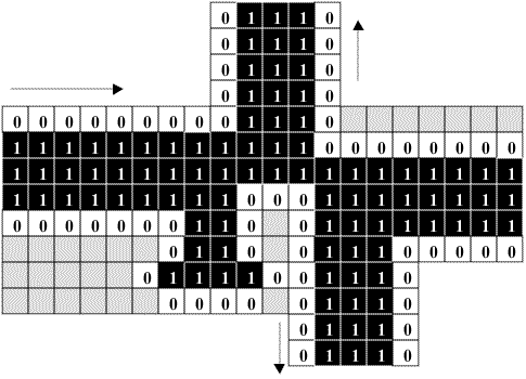
Fig. 3.4.1 Banks' fan-out junction
Although the four arms of the junction are fairly straightforward, I can't imagine how much time it must have taken Banks to devise the configuration where they join in exactly such a way that a signal coming in from the left eventually propagates up, straight ahead, and down. The little "foot" at the left-middle-bottom of the configuration is particularly ingenious, because it is necessary to dampen (extinguish) a stray rebounding signal. Banks used a computer to program simulations of his
CA, but even so it must have been quite tedious.
|
|
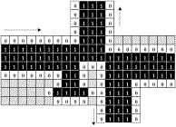
Fig. 3.4.2 Animation of Banks' fan-out junction
(click to open)
|
Here is an animation of how the "signal" will propagate as it approaches the junction from the left, according to Banks' three rules.
[Click here
to open a step-by-step PDF.]
|
|
The fan out junction is not reversible. It is designed to accommodate a signal entering from the west (in this orientation), causing it to fan out into three signals. However, the same is not true of signals entering from the north, east, or south, any of which will simply die out at the junction as though they had hit a dead end. This turns out to be an important feature of the junction when it is later incorporated into Banks' logic circuits.
3.5 The clock.
One of the features of this system that will make the logic gates work properly (as shown later) is that when two signals meet at the junction, they destroy each other, leaving nothing that moves. This is an artifact, a consequence, of the three rules operating in the confined space of the wires. That being the case, Banks needed a reliable way to generate a signal that can meet any incoming signal in order to destroy it when the logic gate requires that
the incoming signal disappear. Banks accomplishes this with a
"clock" that produces signals at regular
intervals.
The clock circuit consists of a signal in a loop, endlessly circulating. At one point in the loop, the signal splits - sending one signal off into the larger machine, and another back into the loop. The number of cycles required to complete a loop is precise and controllable. The following illustration of the clock requires eight steps for a complete loop, but the reader can see that by lengthening or shortening the "arm" of the clock a different timing
interval can be obtained.
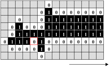
Fig. 3.5.1 Banks' clock configuration
|
| You can diagram out for yourself how this loop will operate. Or you can click on the thumbnail
to the right for an animation.
[Click here
to open a step-by-step PDF.] |

Fig. 3.5.2 Animation of Banks' clock
configuration (click to open)
|
Already, we may begin to sense that Banks' three rules of transition will allow us to manipulate the signal travelling down the wire in any way we wish.
3.6 The logic element.
The basic logic element of Banks' system is a junction that distinguishes among two inputs, such that the output is true (the signal gets through) if one of the inputs is true (there is a signal present) and the other is false. Banks constructs this element from the fan out junction described earlier. He modifies the fan out junction by 1) adding a "bump" to the north arm, which will act like a dead end to kill any signal traveling northward out of the junction; 2) eliminating the south arm of the junction as unnecessary; and 3) adding a peculiar little foot to the west branch, which will capture and destroy a signal traveling westward out of the junction.
If we label the inputs "A" coming from the north, and "B" coming from the west, then this logic element will behave as follows:
1. A solitary signal coming from the north (A) will peter out and be extinguished at the junction.
2. A solitary signal coming from the west (B) will pass through the junction and exit as output.
3. Two signals, coming from both the north (A) and west (B) will meet head on at the junction and die out. They will destroy each other, figuratively speaking.
Here is the configuration of the logic element, and you will see that it is a fan out junction that is missing the southward
leg, and with an added bump on the northward leg (to kill a stray
signal heading north).
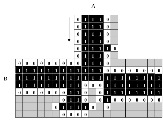
Fig. 3.6.1 Banks' logic element
We may diagram the possibilities in a "truth table." The truth table for Banks' basic logic element sets out the above rules as follows:
|
|
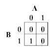
Fig 3.6.2 Truth table of the Banks logic element
|
In this, the top rows represent the conditions that the A input is false ("0," no signal present), or true ("1," signal present). Similarly, the left columns represent the conditions that the B input is false or true. The inside boxes show what the output will be for any combination of these conditions. The only condition for which the output will be true is when A is false (first column) and B is true (second row), i.e., the lower left box that shows a "1."
[note 4.1.1]
|
|
To see how this logic element works, we will animate the three cases described above - A only is present; A and B are both present; and B only is present. (The fourth case, neither A nor B is present, is totally boring because absolutely nothing happens, complete with no output. Only a Samuel Beckett would put in the effort to illustrate such a case.)
|
|
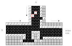
Fig. 3.6.3 Animation of Banks' logic element,
input from A only (click to open)
|
Case I: A input only.
Click on graphic for an animation.
[Click here
to open a step-by-step PDF.] |
|
|
|
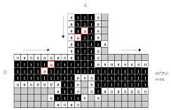
Fig. 3.6.4 Animation of Banks' logic
element, input from A and B (click to open)
|
Case II: A and B both input.
Notice that this arrangement, whereby the A and B signals destroy each other, works only when the signals are synchronized such that they meet exactly head-on. It is trivially easy in principle to achieve such synchronization - one has only to count the number of cells between the origin of a signal and the junction.
[Click here
to open a step-by-step PDF.]
|
|
|
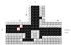
Fig. 3.6.5 Animation of Banks' logic element,
input from B only (click to open)
|
Case III: B input only.
This is the only case in which a signal can get through to the output wire.
[Click here
to open a step-by-step PDF.] |
3.7 The NOT gate.
We see from the above that a signal from A will be destroyed by an incoming signal from B, and that a solo signal from B will pass through to the output wire. All that is needed for a NOT gate, then, is to focus on input A. We will have every signal from input A met by a signal from input B (resulting in an output of false when A is true); and we will have a drone signal from input B that will get through so long as there is no signal from input A (resulting in an output of true when A is false). This will be a logical NOT gate that inverts the signal from A.
|
| With proper synchronization, this can be achieved by attaching a clock to the westward arm of the logic element, input B. The clock will regularly send a drone signal into input B. If there is an A signal to meet the drone signal, both will be destroyed and nothing will pass, yielding an output of nothing/zero/false. On the other hand, if there is no A signal to meet it, the drone signal will pass through to the output, yielding an output of signal/one/true.
Thus, if the A input is true, the NOT gate output will be false; and vice versa, if the A input is false, the NOT gate output will be true. An inversion of the input.
I will not provide a separate animation of this inverting gate because it is incorporated into the next element, Banks'
piece de resistance, . . . |

Fig. 3.7.1 Banks' NOT gate
|
3.8 The NOR gate
You will recall that in order to build a complete general purpose computer, all Banks needs to devise (apart from transmitting wires) is a single logic gate - the NOR gate. Everything else is tinker
toy combinations of NOR gates in this or that configuration. With just the elements discussed previously, Banks is able to build a working NOR gate.
[note 4.2]
|
| You will further recall that a NOR gate operates in such a manner that the output is false if either (or both) of the inputs is
true. The NOR gate's output is true if and only if both of the inputs are false.
|
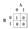
Fig. 3.8.1 Truth table for a NOR gate
|
Accordingly, Banks needs to devise a configuration of cells such that:
- a signal entering the junction from input A only will be destroyed
- a signal entering the junction from input B only will be destroyed
- signals entering the junction from both A and B will be destroyed
- no signals entering the junction at all will produce an output!
This is so trivially easy to accomplish with the elements given previously that Banks doesn't even bother to illustrate it! Go ahead, figure it out. Here is how Banks describes it:
"The NOR function . . . can be constructed from the logic element with a NOT function feeding into the B input."
Banks' statement is completely true, but it took me a long time to verify it. That is, in fact, why I wrote this lengthy commentary. In fact, this entire essay is leading up to my triumphant animation of Banks' NOR gate, which is a clock leading into a Banks logic element (making a NOT gate) leading into another Banks logic element from the west. This is what it looks like:
|
|
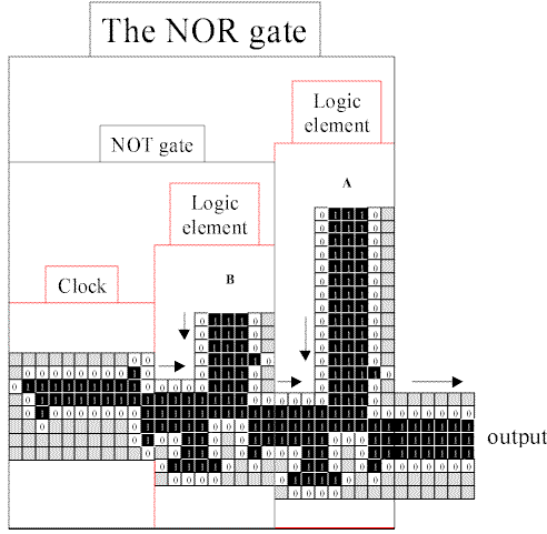
Fig. 3.8.2 Banks' NOR gate
And this is how it works:
|
|
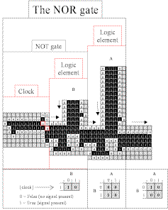
Fig. 3.8.3
Animation of NOR gate, both inputs false (click to open)
|
NOR gate Case I: A is false (no input) and B is false (no input). Output is true (because of the clock signal).
[Click here
to open a step-by-step PDF.]
|
| NOR gate Case II: A is true and B is false (no input). Output is false (because the clock signal meets and destroys the signal from A).
[Click here
to open a step-by-step PDF.]
|
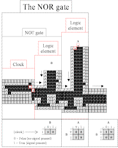
Fig
3.8.4 Animation of NOR gate, A input only (click to open)
|
|
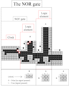
Fig. 3.8.5
Animation of NOR gate, B input only (click to open)
|
NOR gate Case III: A is false (no input) and B is true. Output is false (because the clock signal meets and destroys the input from B).
[Click here
to open a step-by-step PDF.]
|
| NOR gate Case IV: A is true and B is true. Output is false (because the clock signal meets and destroys input from B, and the input from A self-destructs).
[Click here
to open a step-by-step PDF.]
|
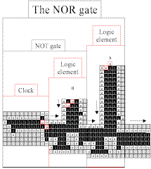
Fig.
3.8.6 Animation of NOR gate, input from both A and B (click
to open)
|
| That's it for Banks' infinitely configured, two-state, five neighborhood, two-dimensional universal cellular space that can act like a general purpose universal computer. That's how he did it.
Next and finally, we will briefly consider what it all means.
|
Endnotes
4. Each of the other possible combinations of
the values of the relevant five cells could also be written as a rule
that would result in a "transition" to the cell's same
value, i.e., a transition without a change. It is somewhat useful to
think of things this way, because the cell must decide on its next
value regardless of whether that value will be the same or different
compared to its present value. However, the fundamental yes/no logic
operation makes it so easy to ignore the "no change"
results. (Does the five-bit data set match one of the three transition
rules? Yes/no. If yes, then change your value; if no, then don't
change your value.)
4.1. One of the consequences of this
"handedness" of the wire is that special provision must be
made for ensuring that a signal arrives at its destination on the
proper side of the wire. For example, if we wish to have the
wire-signal make a right hand turn, we must consider which side of the
incoming wire is carrying the signal; and which side of the outgoing
wire must carry it further. Banks puts in a great deal of effort
to create the special "curves" necessary to achieve the
desired outcomes -- inside-to-inside right turn; inside-to-outside
left turn; and so forth. The end result -- a working computer --
cannot be achieved with a single wire running in a straight line.
4.1.1 Banks' universal logic element bears a
similarity to the XOR gate
mentioned in Part 1, but it is even more exclusive. The XOR gate
is true if one of the inputs is true and the other is false. However,
Banks' logic element discriminates between the two inputs, A and
B. It operates as a B-and-NOT-A gate, which is the only true
case. The other true case for the XOR gate (NOT-B-and-A) is
false for the Banks gate. It is known that the XOR gate cannot
act as a universal gate like the NAND and the NOR. Curious,
then, that a B-and-NOT-A gate can do so.
4.2. These illustrations focus only on the
logic gates themselves. Of course, additional components such as
the curves discussed above at note 4.1 must be used to create the full
computer. Also, Banks had to devise a "crossover" that
would allow the wires to cross and signals to pass through without
change. The crossover he created consists of a curious
configuration of three NOR gates that together shepherd the crossing
signals past each other (see
Banks71 at 25). This would be quite complicated to illustrate,
so I
leave it to the reader to investigate further.
|
|
|
 |

|
|
| © Copyright 2004 by Ross Rhodes. |
|

|
|